Inventors with similar research interests:
Location History:
- Yorktown Heights, NY (US) (2008 - 2012)
- Schenetady, NY (US) (2015)
- Schnectady, NY (US) (2015 - 2017)
- Schenecatady, NY (US) (2017)
- Albany, NY (US) (2010 - 2019)
- San Jose, CA (US) (2022)
- Schenectady, NY (US) (2013 - 2024)
Company Filing History:


Years Active: 2008-2025
Areas of Expertise:
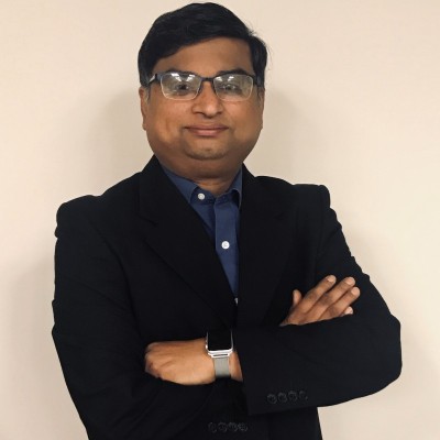
Title: Veeraraghavan S Basker: A Mastermind in Semiconductor Innovations
Introduction:
Veeraraghavan S Basker, based in Schenectady, NY, is an exceptional inventor and innovator in the field of semiconductor devices. With an impressive portfolio of 428 patents, Basker has made significant contributions to the technological advancements in this domain. This article sheds light on his latest patents, career highlights, collaborations, and his invaluable contributions to the field.
Latest Patents:
Basker's recent patents showcase his expertise in semiconductor device manufacturing and design. One notable invention is the "Source and Drain Contact Cut Last Process to Enable Wrap-Around-Contact." This technique involves the formation of a silicide layer between a source/drain contact liner and the source/drain regions through annealing. It also utilizes a block layer to protect and preserve the desired regions, resulting in efficient and effective semiconductor device manufacturing.
Another groundbreaking patent by Basker is the "Hybrid Diffusion Break with EUV Gate Patterning." This invention provides a solution for preventing contact between adjacent nanosheet devices while maintaining uniform gate widths. By incorporating a diffusion break with a larger width, this innovation helps enhance the performance and reliability of semiconductor devices.
Career Highlights:
Basker has honed his expertise while working with industry giants such as IBM and GlobalFoundries Inc. Throughout his career, he has consistently pushed the boundaries of semiconductor technology, leading to numerous breakthroughs and advancements. His work has greatly influenced the field, inspiring fellow researchers and shaping the future of semiconductor device design.
Collaborations:
Collaboration often drives innovation, and Basker's work is no exception. He has collaborated with esteemed individuals, including Kangguo Cheng and Junli Wang. Together, they have combined their expertise to bring forth novel solutions in semiconductor manufacturing, enabling the industry to progress further.
Conclusion:
Veeraraghavan S Basker stands as a luminary in the world of semiconductor innovations and patents. With an impressive array of 428 patents, his contributions have significantly impacted the field's advancements. Basker's expertise, combined with his experience at renowned companies like IBM and GlobalFoundries Inc., has paved the way for cutting-edge semiconductor device manufacturing techniques. Through his collaborations, Basker has further reinforced the importance of teamwork and knowledge sharing in driving technological progress. His contributions will continue to be instrumental in shaping the future of semiconductor technology.
